42 ic 7400 pin diagram
The minimized boolean expression is then converted into logic gate diagram which is built on a breadboard using 7400 series ICs. The following logic gate ICs are used in the construction of the circuits – 7408 IC – The 7408 IC has quad 2-input AND gates. The IC has the following pin configuration – Fig. 7: Circuit Diagram of Excess 3 to BCD Code Converter The IC has the following Pin ... IC 7400, 7408, 7432, 7447, 7404. Ø IC 7400. IC TTL Seri 7400 adalah kumpulan IC-IC yang turut berperan penting dalam sejarah IC dan penyebarannya. Walaupun telah beredar cukup lama, namun versi-versi modern dari Seri 7400 ini tetap masih digunakan hingga sekarang ini. Pada awalnya, seri 7400 dibuat dengan Transistor bipolar.
NAND gate (IC 7400), NOR gate (IC 7402), X-OR gate (IC 7486), Power supply, Digital IC trainer kit, connecting wires. BOOLEAN EXPRESSIONS . CIRCUIT DIAGRAM Pin Identification. Figure (a) Integrated circuit . Note: The chip must be inserted in the bread board in such a way that the identification mark should be on our left side. In this position ...

Ic 7400 pin diagram
22.10.2021 · In the original 7400 series TTL parts it was common to have an output that was able to SINK 16 mA while maintaining the output at a valid logic '0'. A TTL input would source 1.6 mA into a low output and was referred to a 1 Unit Load. So the output capability was capable of driving 10 Unit Loads. The IC 7400 is a 14-pin chip and it includes four 2-input NAND gates. Every gate utilizes 2-input pins & 1-output pin, by the remaining 2-pins being power & ground. This chip was made with different packages like surface mount and through-hole which includes ceramic (or) plastic dual-in-line and flat pack. ic- 7400 IC 7400 Pin Configuration. The pin configuration of 7400 IC is discussed below ... Pin Diagram: Truth Table: IC 7402; It is a quad two inputs NOR Gate. All these gates may be used independently. On any gate with either input 'High' the output is low. When both the input are 'Low' the output is 'High'. Pin Diagram: Truth Table: IC 7404: It is a two input NOT Gate also known as Hex Inverter.
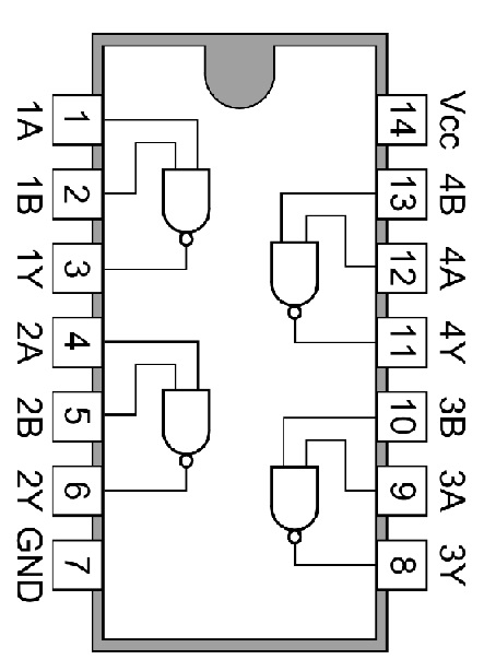
Ic 7400 pin diagram. The first part number in the series, the 7400, is a 14-pin IC containing four two-input NAND gates. Each gate uses two input pins and one output pin, with the remaining two pins being power (+5 V) and ground. This part was made in various through-hole and surface-mount packages, including flat pack and plastic/ceramic dual in-line. Additional characters in a part number identify the package ... IC-7400/7410 IC-7600/7700/7800 IC-9100: Notes **Speaker audio (usually Pin #8) and power ... If the SignaLink is attached to your radio's 8-pin Round Mic Jack, then please see the diagram above under "8-Pin Round MIC Connector". JP-1. Pin-out Pin 1 - RTTY or N/C Pin 2 - Ground Pin 3 - Send Pin 4 - Mod In Pin 5 - AF Out Pin 6 - Squelch Pin 7 ... IC 556 IC 555 LM3914 LM34dz TDA2005 Ixdf404SI 16pin IXDI404SI-16pin IXDN404SI 16pin IXDIF404 8pin IXDI404 8 Pin SOIC IXDN404 8 Pin SOIC TDA7272 8085 Pin Diagram TDA7273 TDA7274 L6219 UDx2916 L293 LMD18200 SN754410 AD9573 AAT3128 TB2901H TDA1301 TDA1085CD TDA10046 DVB T-Channel Receiver TD7626F,TD7626FN 4N25 16f84 16F88 16f628 16F877 18F452 ... Pin Functions (continued) PIN I/O DESCRIPTION NAME CDIP, CFP, SOIC, PDIP, SO, SSOP SO (SN74xx00) CFP (SN5400) LCCC 3Y 8 — 8 12 O Gate 3 output 4A 13 — 12 18 I Gate 4 input 4B 12 — 13 19 I Gate 4 input 4Y 11 — 14 16 O Gate 4 output GND 7 4 11 10 — Ground NC — — — 1, 5, 7, 11, 15, 17 — No connect VCC 14 8 4 20 — Power supply
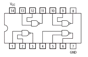
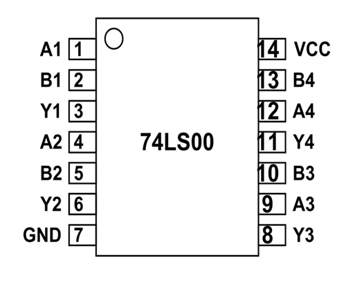
74LS02 is a LOGIC GATE IC and member of 74XXYY IC series which are logic gates. There are four NOR gates in the IC and each gate has two inputs, hence the name QUADRUPLE TWO INPUT NOR GATE. The gates in the chip are designed by low power SCHOTTKY TRANSISTORS. 74LS02 Pin configuration. 74LS02 is a 14 PIN IC as shown in the pinout diagram. The ... 1.6.2018 · Logi7400. Logisim 7400 series integrated circuits library.. Variants. There are two variants of the library with different circuit appearances available: In the classic Logi7400dip library, the circuit appearance reflects the physical pin layout of the DIP packaged chips.; The new Logi7400ic library provides a logical circuit appearance.; Goal. This library aims to be a comprehensive 7400 ... Photocell Circuit Diagram. The photocell used in the circuit is named as dark sensing circuit otherwise transistor switched circuit.The required components to build the circuit mainly include breadboard, jumper wires, battery-9V, transistor 2N222A, photocell, resistors-22 kilo-ohm, 47 ohms, and LED.. The above photocell circuit works in two conditions like when there is light and when it is dark. 7400 IC Chip Circuit Diagram 7400 package and pins showing pin outs . Here is some information about the 7400 Series TTL Integrated Circuits: PIN 2 PIN 3 PIN 1 PIN 4 PIN 5 PIN 6 PIN 13 PIN 12 PIN 11 PIN 10 PIN 9 Ground, PIN 8 PIN 7 PIN 14, +5 volts Dot near pin 1 or Notch at top center Top View of a 14 pin 74xx device ...
The 555 timer IC is an integrated circuit (chip) used in a variety of timer, delay, pulse generation, and oscillator applications. Derivatives provide two or four timing circuits in one package.It was commercialized in 1972 by Signetics. Numerous companies have made the original bipolar timers and similar low-power CMOS timers too. In 2017, it was said over a billion 555 timers are produced ... Input b. Select c.Strobe d. Output 2. Gambarlah diagram pin dari IC 74153! 3. Gambarlah diagram koneksi rangkaian multiplekser data 2 ke 1 menggunakan IC 7400! 4. Gambarlah diagram koneksi dari rangkaian decade counter yang menghasilkan 4 keluaran yaitu pembagi frekuensi (PF) 2, PF 4, PF 8 dan PF 10! 5. Gambarkan diagram koneksi rangkaian ... Here we had designed 4-line to 16-line decoder using two popular TTL IC 7400 and 7422. As we know that 7422 is 4-line to 10-line decoder thus we had used two 7422 IC. IC 1 can only decodes the 4-bit input to 10 ten lines 0 through 9 in conventional manner rest 6 line is obtained from IC 2. Pin 3 to 7 and 9 pins only goes high rest of pin are ... TOP WIEWED Pin A1 index , 7400 ) is the first implementation of the fourth (G4) full implementation of the PowerPC Reduced , 7400 microprocessor design is ...
Practical Demo Of S R Latch Using 7400 Nand Gate And Push Button Switches Funny Electronics
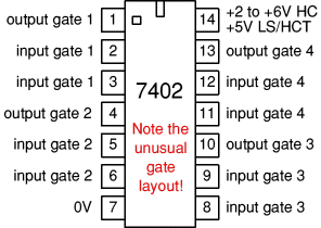
Pin 6 is the second input Pin of the Second NOR gate in IC. GND: Pin 7: Pin 7 will be used as the common ground by all the devices and power supply used with the IC to make the ground common. 3A: Pin 8: Pin 8 will be used as the First input pin of the third NOR gate in IC 74LS02. 3B: Pin 9: Pin 9 will be the second input pin of the third NOR ...

Pin On My Collection
IC 7408 is a logic gate IC. It consists of four two-input AND Gates. The IC 7408 has total fourteen pins including ground and Vcc. The simple pin diagram is shown here. The internal structure of IC 7408 described here. Pin Description of IC 7408 explained in detail. Application of IC 7408 given here.
1
7400, 7400 Datasheet, 7400 Quad 2-Input NAND Gate, buy 7400, ic 7400. ... Pin Layout. TTL 7400 Pin Layout. Pin Description ...
Simple Circuits Using Ic 7400 Nand Gates Homemade Circuit Projects
20.12.2011 · •You must learn to recognize which pin is Pin one on the ICs. The dot in the corner of the chip designates pin 1. This is true on the schematic symbol and on the actual IC. Count down, up, and across from pin 1. –Look at the next slide to see if you can …

Logic Gate Ic S Concise Information And Various Applications Of Logic Gate Ic S
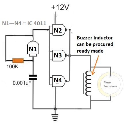
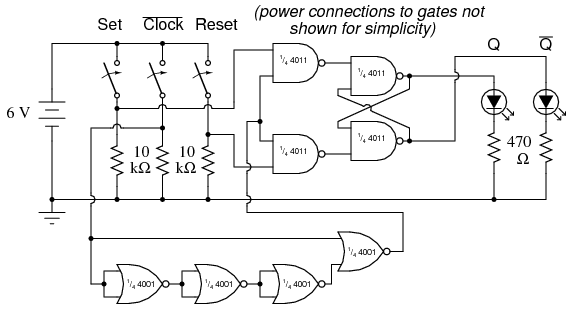
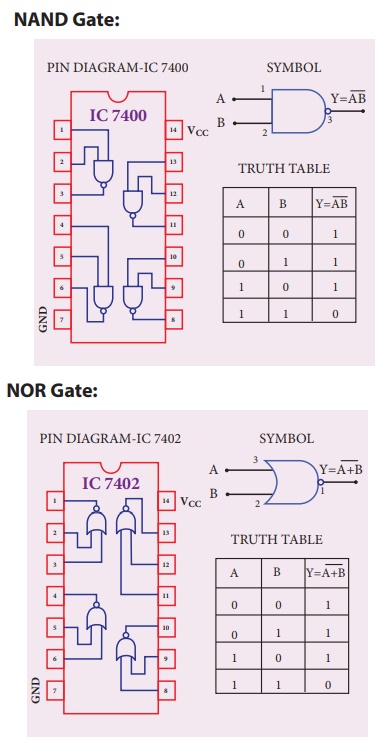
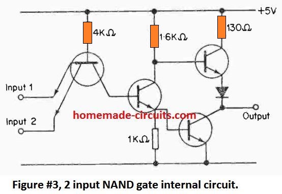
PIN configuration diagram 5 NAND GATE. Circuit diagram and working of NAND gate. PIN Configuration diagram of Logic Gates 1 NOT GATE. The IC 7400 consist of four NAND Gates. Any of the two chips can be. The IC requires a supply voltage of 5V which can be tolerated up to 7V. Pin 7 is the ground pin that provides power to the chip.
Pc Cp220 Digital Integrated Circuits Introduction
How to succeed in bad times: https://my-store-11692020.preview.teespring.com/listing/how-to-succeed-in-bad-times#previewData=U2FsdGVkX19zrbZUqQ7o+Bv7BcBA5571...
Simple Circuits Using Ic 7400 Nand Gates Homemade Circuit Projects
Draw the pin diagram of IC 7400. digital electronics; class-12; Share It On Facebook Twitter Email. 1 Answer +1 vote . answered Mar 16, 2020 by Mohit01 (54.3k points) selected Mar 16, 2020 by Richa01 . Best answer. The pin diagram of IC 7400 is: ← Prev Question ...

Building Multiplexer And Demultiplexer Using Sn 7400 Series Ics De Part 16
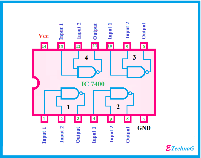
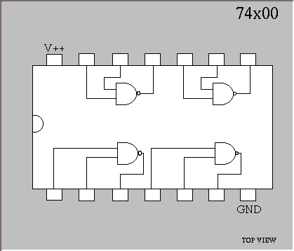
A 7400 consists of four NAND gates, with 2 input pins and 1 output pin for each of the gates, and also a pair of pins for the power supply inputs, pin 14 and pin 7. IC 7400 Family The other members of the 7400 family may come with higher number of input pins such as 3 input NAND gates, 4 input NAND gates and the 8 input NAND gate featuring more input combination options for each gate.

File 7400 Quad 2 Input Nand Gates Png Wikimedia Commons
manufacturer’s microphones have different pin assign-ments, and connection to the IC-7400 may damage the transceiver. WORD DEFINITION RWARNING Personal injury, fire hazard or electric shock may occur. CAUTION Equipment damage may occur. NOTE If disregarded, inconvenience only. No risk or personal injury, fire or electric shock. IC-7400.qxd 01.12.27 13:09 Page 2. ii SUPPLIED ACCESSORIES The ...

List Of 7400 Series Integrated Circuits Wikipedia
Pin diagram of IC 7400 explained here. Figure 35 is a functional block diagram of the therm timer therm limit and its associated circuitry. Every gate utilizes 2-input pins 1-output pin by the remaining 2-pins being power ground. The counter has a gated zero reset and also has gated set to-nine inputs for use in BCD nines complement.
Ic 7400 Pin Configuration Circuit Specifications And Its Applications
P. Marian. 7400 IC is a Quad 2-Input NAND Gate that contains four independent gates each of which performs the logic NAND function. SN74LS00 datasheet. DM74LS00 datasheet. 7400 IC Circuit Diagram. 7400 package and pins. No related posts. Previous. 555 Timer Design Software.
Solved Given The Logic Diagrams For The 74161 Binary Chegg Com
If the SignaLink is attached to your radio's 8-pin Round Mic Jack, then please see the diagram above under "8-Pin Round MIC Connector". JP-1 Pin-out Pin 1 - RTTY or N/C Pin 2 - Ground Pin 3 - Send Pin 4 - Mod In Pin 5 - AF Out Pin 6 - Squelch Pin 7 - +13.8V Pin 8 - ALC Radio Models IC-275A IC-707 IC-725/728/729 IC-735/736/737 IC-7400 IC-746 ...
Simple Circuits Using Ic 7400 Nand Gates Homemade Circuit Projects
3.5.2016 · Connect 8 individual wires to the ON side array & connect it numbered from 1 to 8 to Q terminals of IC 74682 (8 bit magnitude comparator) from Q0 to Q7 (Refer the pin diagram uploaded). Here’s where we have to do a little sacrifice, we may only use the 4 bits of the T – flip-flops in the 1 – 12 counter. 3 more bits from the 0 – 5 counter of the minutes & 1 bit for A/P.

Ic 7400 With Sdr Panadapter From Tsp S R L Www Tspelettronica Com
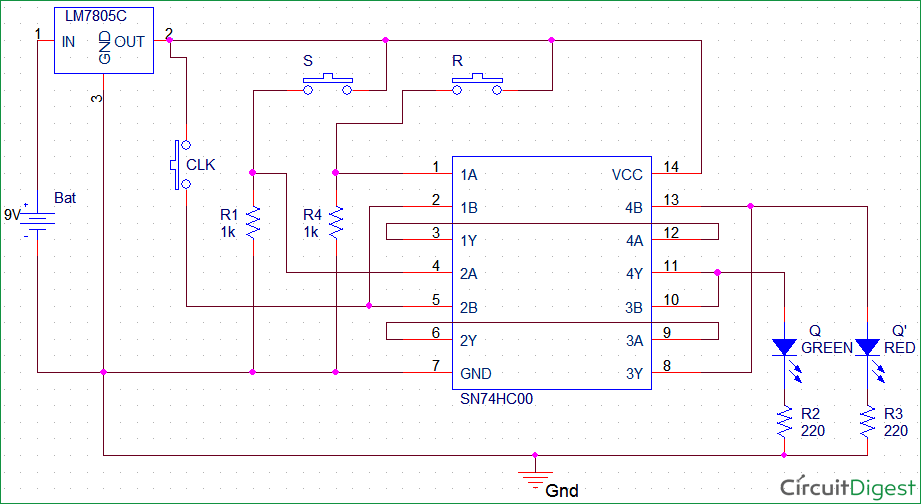
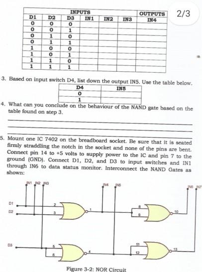
2. Place the IC in the board so that pin 1 should be on the upper left of the board. Half of the legs should be on one side of the pink gap and half on the other. 3. Connect pin 14 of the IC chip to Vcc and pin 7 to ground. 4. Connect pin 1 and 2 of the IC chip to the input (you can take the input from the two top
74 Series Logic Ics Electronics Club
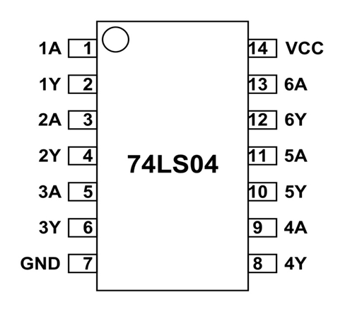
Pin-out diagram of 7404 NOT gate IC. Each 7404 NOT gate IC has 6 NOT gates arranged as shown in the following figure. 14th pin is the Vcc and the 7th pin is the Ground. The outputs directly interface to CMOS, NMOS and TTL. It supports wide operating conditions and has large operating voltage range.
74ls04 Pinout Features Equivalent Examples Datasheet
12+ Nand Gate Ic Pin Diagram. How do you make one? Nand gates are available in the ic packages. 7400 IC Quad 2 input positive NAND Gate 74HC00 74LS00 … from secureservercdn.net. An ic chip containing nand gates. So with two buttons we can realize the truth table of nand gate. See the newest logic products from ti, download logic ic datasheets ...
Github Rishabhc32 Flip Flops Making Flip Flops And Latch Using Nand Gates
Nederlands: Deze categorie is alleen voor ic-pinconfiguraties. Voor functieschema's is er de categorie: IC functional diagrams, en voor foto's: Close-ups of integrated circuits. Het SVG -formaat heeft de voorkeur voor alle schema's in deze categorie. Русский: Эта категория предназначена исключительно ...
Simple Circuits Using Ic 7400 Nand Gates Homemade Circuit Projects
Mar 26, 2020 - IC 7400 is fourteen pin Logic Gate IC. The IC 7400 consist of four NAND Gates. Pin diagram of IC 7400 explained here. Operating Condition and Electrical Characteristics of IC 7400 described here. The Internal Structure and Pin Description of IC 7400 explained detail. Application of IC 7400 given here.
1
IC 7400 is fourteen pin Logic Gate IC. The IC 7400 consist of four NAND Gates. Pin diagram of IC 7400 explained here. Operating Condition and Electrical Characteristics of IC 7400 described here. The Internal Structure and Pin Description of IC 7400 explained detail. Application of IC 7400 given here.
Simple Circuits Using Ic 7400 Nand Gates Homemade Circuit Projects
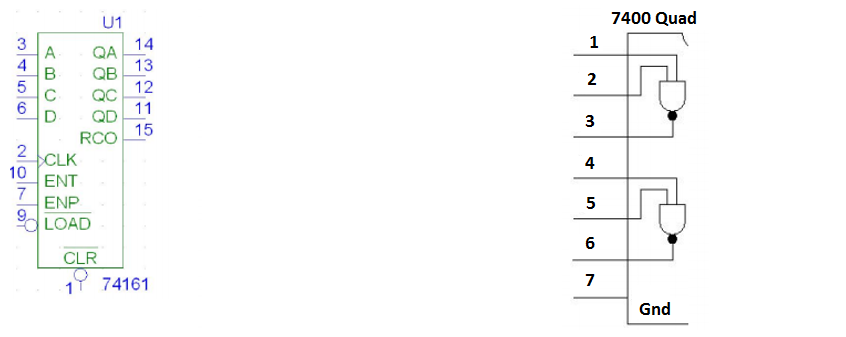
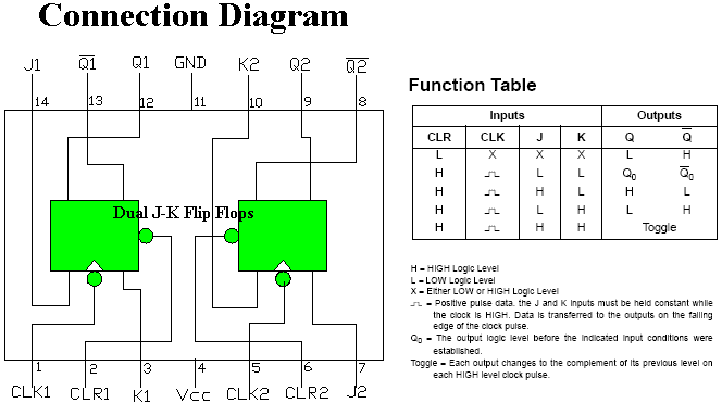
Pin 5 is used as the power pin. It is used to power up the IC to make it functional. 2 CLK: Pin 6: Pin 6 is an input pin. It is used to give the clock pulse to the clock of the second JK flip flop. HIGH to LOW pulse will only affect the IC. 2 PRE' Pin 7: Pin 7 is a preset input pin of the second flip flop.
Ic 7400 Pin Configuration Circuit Specifications And Its Applications
Pin Diagram: Truth Table: IC 7402; It is a quad two inputs NOR Gate. All these gates may be used independently. On any gate with either input 'High' the output is low. When both the input are 'Low' the output is 'High'. Pin Diagram: Truth Table: IC 7404: It is a two input NOT Gate also known as Hex Inverter.

7400 Series Integrated Circuits Wikipedia
The IC 7400 is a 14-pin chip and it includes four 2-input NAND gates. Every gate utilizes 2-input pins & 1-output pin, by the remaining 2-pins being power & ground. This chip was made with different packages like surface mount and through-hole which includes ceramic (or) plastic dual-in-line and flat pack. ic- 7400 IC 7400 Pin Configuration. The pin configuration of 7400 IC is discussed below ...

Electronics 7400 Chip
22.10.2021 · In the original 7400 series TTL parts it was common to have an output that was able to SINK 16 mA while maintaining the output at a valid logic '0'. A TTL input would source 1.6 mA into a low output and was referred to a 1 Unit Load. So the output capability was capable of driving 10 Unit Loads.

7400 Quad 2 Input Nand Gate 74hc00 Integrated Circuit Ic Electronics Introduction Youtube
Lessons In Electric Circuits Volume Vi Experiments Chapter 7
Simple Circuits Using Ic 7400 Nand Gates Homemade Circuit Projects
1
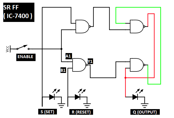
Sr Flip Flop Circuit Diagram With Nand Gates Working Truth Table Explained
74ls00 Pinout Configuration Equivalent Circuit Datasheet

7400 Datasheet

Building Encoder And Decoder Using Sn 7400 Series Ics De Part 15
Verification Of Truth Tables Of Logic Gates Using Integrated Circuits Physics Practical Experiment

Ic 7400 Pin Diagram Circuit Design Datasheet Application Etechnog
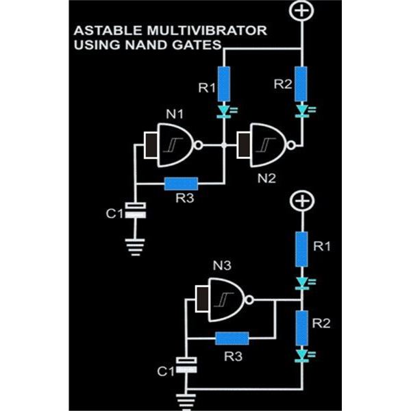
Make This Astable Multivibrator Blinker Circuit Using Nand Gates Under Repository Circuits 27408 Next Gr
Solved Materials Needed 1 Pc Ic 7400 Quadruple 2 Input Chegg Com
Ic 7400 Pin Diagram Circuit Design Datasheet Application Etechnog
Simple Circuits Using Ic 7400 Nand Gates Homemade Circuit Projects
7400 Series Ttl Ic S 7400 7449

74hc00 74hct00 Quad 2 Input Ttl Nand Gate Pinout Diagram Funny Electronics
7473 Dual Master Slave J K Flip Flops With Clear And
Ic7400 Nand Gate Youtube
Simple Circuits Using Ic 7400 Nand Gates Homemade Circuit Projects


Comments
Post a Comment